 |
 |
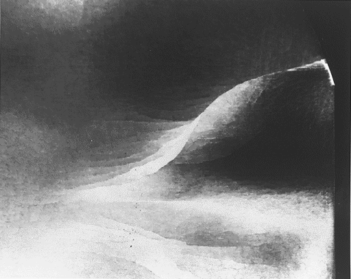
X-ray topography reveals the intricate defect structure of crystals. Topographs of single crystal wafers of GaAs used in the manufacture of high speed circuits often reveal two common crystal defects: a cellular dislocation network and low angle grain boundaries. This topograph captures a rare instance which shows that the two dislocation types are not distinct. The cell boundaries of the cellular dislocation network can cooperatively give rise to a much larger low angle grain boundary, and in this instance do so in a very interesting and aesthetically pleasing way.
(Quill, stylus, plume, feather, spray)