 |
|
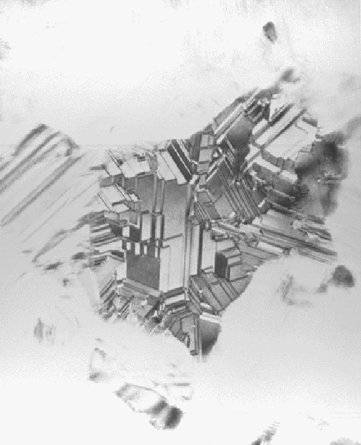
High-purity polycrystalline silicon ("polysilicon") films, produced by low pressure chemical vapour deposition at elevated temperatures, are a common component of microelectronics semiconductor devices. Because of their importance, considerable research has been carried out in order to understand the physical nature, of these films. One technique that is being used increasingly for studies of semiconductors is transmission electron microscopy (TEM), which permits examination of specially thinned samples in much the same way that thin biological sections are examined by optical microscopy.
The micrograph shown here was from an area of polysilicon that had been reduced to less than one ten thousandth of a millimeter in thickness. It shows an individual crystallite at high magnification. The specimen had to be tilted with an accuracy of 0.1 degree, in order to reveal the microstructure, showing that the crystallites contained a high density of defects known as microtwins. Some of the microtwins were only a few atoms thick. MAGNIFICATION X1.5 MILLION